With the importance of semiconductors only increasing across multiple industries, a new facility in Scotland could help bolster the value chain in the crucial aspect of packaging.
Demand for advanced semiconductor packaging is growing rapidly in parallel with the development of next-generation technologies, including artificial intelligence (AI), photonics, quantum, and integrated sensing systems. The complexity of devices heightens the importance of advanced packaging for demanding applications.
“Semiconductor packaging is no longer viewed as a passive protection mechanism,” says Dr Gladys Benghalia, head of programmes in electrification manufacturing at the National Manufacturing Institute Scotland (NMIS). “It has evolved into an enabling platform – the convergence point for multiple advanced technologies. We’re seeing the integration of materials, design and functionality, where the package defines the system-level architecture. It’s within the packaging domain that we can now engineer performance, power efficiency, thermal management and cost trade-offs at the device level.”
The global growth of advanced semiconductor packaging
In an ever-more connected world, myriad technologies rely on semiconductors. By 2029, GlobalData predicts the global semiconductors market will be worth $993.3bn, growing by 63.2% from 2024. By 2030, the global market value could easily top $1trn.
The global semiconductor manufacturing market is dominated by the Asia-Pacific, which had a 74.4% share in 2024. Within this, China and Taiwan are both prominent manufacturing locations.
However, the three-year shortage of semiconductors from 2020-23 exposed the flaws in existing supply chains being over-reliant on too few locations. Alongside this, geopolitical tensions and supply chain disruptions of recent years have forced nations to focus on more resilient domestic production capabilities.
Furthermore, faster innovation is required for semiconductor packaging capabilities to keep up with specialist demands. Meeting complex requirements can be challenging for the high-volume production models prevalent across South East Asia. If semiconductor packaging lines are unable to provide advanced solutions for next-generation technologies, the innovation curve will be restricted, and opportunities to develop vital solutions will be missed.
The UK is well-positioned to develop such capabilities and contribute to the global value chain, removing the reliance on international suppliers for key components. UK semiconductor packaging is growing at a compound annual growth rate of almost 11%. In line with this growth, the global packaging market is also expanding.
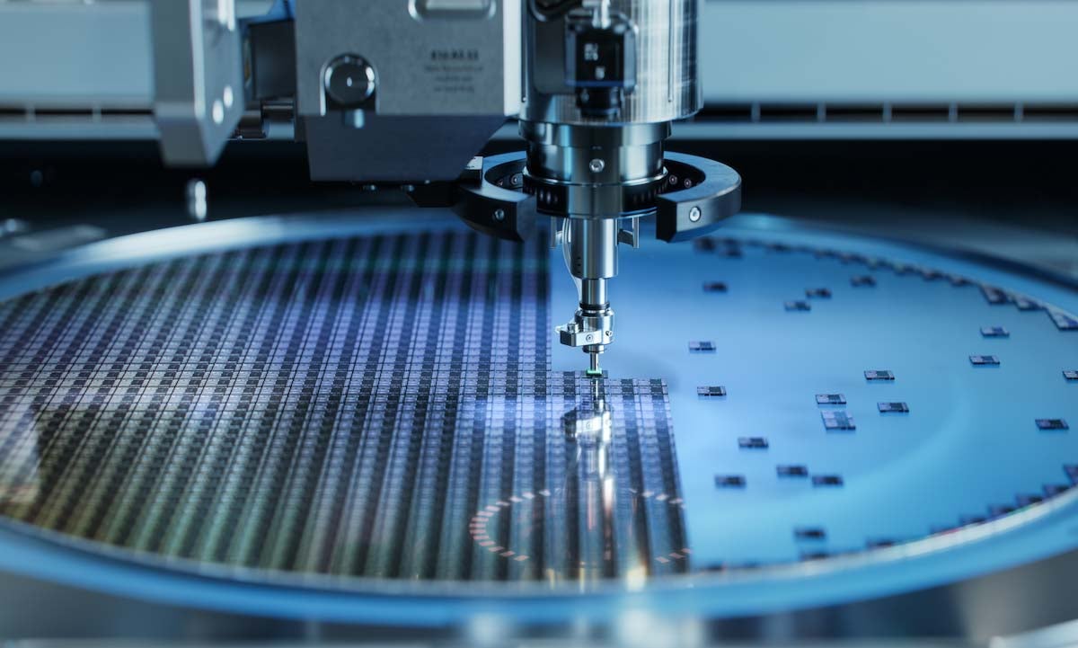
For semiconductors, the packaging is an essential aspect that goes far beyond mere encapsulation and Scotland is developing specialist capabilities in this essential area.
“We’re developing packaging solutions that actively define system behaviour, rather than just simply housing chips,” adds Benghalia.
Advanced semiconductor packaging facility in Europe
At the forefront of tech innovation in Scotland is the National Advanced Semiconductor Packaging and Integration Centre (NASPIC), which was officially announced in July and is a key facility in meeting increased demand. Based near Glasgow Airport, NASPIC is the first open-access facility of its kind in Europe and will support accelerated development timelines of semiconductors, providing packaging in a matter of days instead of months.
The National Manufacturing Institute Scotland (NMIS) is the driving force behind NASPIC, which will be integral to the Advanced Net Zero Innovation Centre (ANZIC) at the University of Strathclyde. Over the next decade, NASPIC is projected to enable £800m in revenue for UK and international businesses and support 300 jobs.

NASPIC is a national hub for advanced semiconductor packaging development, benefiting from a portion of the £160m investment from the UK Government across projects in the Glasgow City Region Innovation Zone (GCRIZ).
NASPIC received an £8m grant from Innovate UK’s Driving the Electric Revolution (DER) Challenge, alongside investment from Scottish Enterprise, for advanced packaging in power electronics. To further capabilities, GCRIZ and Scottish Enterprise are planning to invest a further £29m to expand the leading-edge facilities into photonics, RF, quantum computing and high-performance compute/AI built on advanced CMOS technologies.
The new facility will have the capacity to support both UK and global customers, offering lab-to-line advanced semiconductor packaging components for critical applications.
While NASPIC cannot compete with the major manufacturers of South East Asia in terms of volume, the Scottish site has an edge in providing high-value sovereign assembly prototyping.
“At NASPIC, we are accelerating the prototyping and scale-up of advanced packaging assemblies so innovation can flow rapidly into manufacturing in an industry that’s evolving at extraordinary speed,” saysBenghalia.
UK semiconductor packaging capabilities
UK wafer fabs typically use offshore providers of semiconductor packaging, which can delay development timelines by months and expose manufacturers to supply chain disruption.
Production in the UK will support domestic manufacturing and help to better insulate against supply chain disruption and geopolitical events. Beyond Scotland, the facility offers international semiconductor companies the opportunity to develop low-volume, high-value solutions for complex tech needs that are only possible in a few locations globally.
State-of-the-art equipment at NASPIC will provide partners with full capability across the advanced packaging workflow, from wafer preparation, dicing and die attach, through interconnect, encapsulation and assembly, to subsystem integration and testing.
“Our approach allows companies to truly understand how their technology will scale, not just whether it works in principle,” adds Benghalia. “It’s a distinctive strength of the University of Strathclyde and NMIS: integrating research, development and manufacturing capability, giving our partners the confidence to scale new technologies into real-world applications.”
The pilot production environment enables partners to prove and qualify packaging across areas such as power electronics, photonics, radio frequency (RF), advanced complementary metal-oxide-semiconductor (CMOS), and high-performance computing.
NASPIC has also attracted interest from manufacturers in South East Asia due to the capacity for research and innovation that is not as prominent in high-volume production locations.
“We’re not doing research that simply advances knowledge, we’re closing the gap between innovation and industrial adoption, ensuring new technologies can move confidently from the lab to line,” says Benghalia.
The ambition of Scotland in critical technologies
The long-term ambition behind the facility is to establish Glasgow as a recognised centre of excellence in the ultra-specialist field of advanced semiconductor packaging. Collaborations are at the centre of Scottish innovations at NASPIC, established in partnership with the Compound Semiconductor Applications (CSA) Catapult, while complementing capabilities at James Watt Nanofabrication Centre (JWNC), which can produce sensors, lasers and qubits, for example, for integration into the packages.
The facilities and partnerships are integral to Scotland’s growth strategy in its Critical Technologies Supercluster, connecting the country’s world-class universities with businesses and government.
“Scotland’s ecosystem is incredibly rich, and the Critical Technologies Supercluster is a perfect example. It connects our national strengths in photonics, quantum, semiconductors and sensing and connectivity, bringing together over 150 companies to accelerate cross-sector innovation and industrial growth,” adds Benghalia.
The supercluster was announced in November 2024, with the technologies in the four areas estimated to be worth £4.2bn in sales.
With its foundations in research, the ambition for the supercluster is anticipated to achieve a combined turnover of £10bn by 2035 and is projected to result in the creation of 6,600 additional skilled jobs.
There are notable crossovers between the four pillars of the Critical Technologies Supercluster, which has been established to foster collaboration, boost investment, and expand skills of the developing workforce. These factors all position Scotland strongly to achieve future growth in critical technologies and optimise market opportunities in the tech economy.
To learn more about the development of Scotland’s Critical Technologies Supercluster, download the document below.